Source page: McKinsey & Company
Commentary
Stacking chips
Semiconductors | Manufacturing | Industrials & Electronics
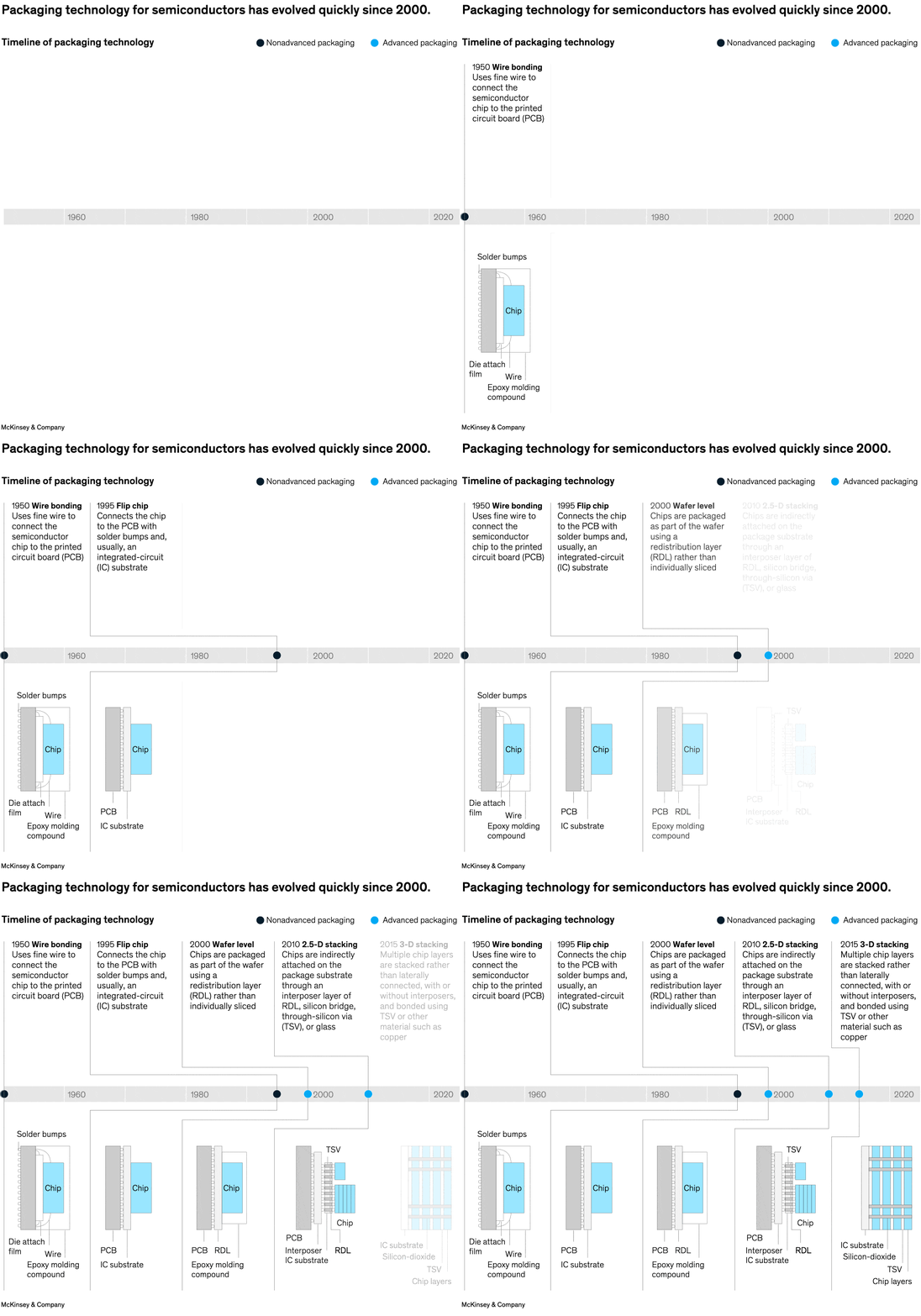
June 26, 2023 – As 5G, autonomous vehicles, and other emerging technologies shape the future of semiconductor demand, advanced packaging for semiconductor wafers could be key to creating value for manufacturers, according to research by senior partner Ondrej Burkacky and coauthors. Since 2000, three major advanced-packaging techniques have become commercially available and offer promising solutions for higher-performing chips: wafer level, 2.5-D stacking, and 3-D stacking.
To read the article, see “Advanced chip packaging: How manufacturers can play to win,” May 24, 2023.
customizer here
Visual form
Technology timeline diagram.
Layout / body structure
A horizontal timeline spans from the 1950s to the 2020s, and the reader follows it left to right as packaging methods appear along the line with annotated illustrations.
What is being compared
It compares nonadvanced and advanced semiconductor packaging approaches across time, showing when major methods such as wire bonding, wafer-level packaging, 2.5-D stacking, and 3-D stacking entered commercial use.
Measurement system
The graphic is organized by time rather than by a numeric value axis, with the legend distinguishing nonadvanced packaging from advanced packaging through color.
Visible structure inside the graphic
The chart uses a central timeline, circular markers placed at different decades, text callouts naming the packaging methods, and small technical illustrations that show how chip components are arranged.
Main takeaway from the visual
The visual makes the pace of packaging innovation visible by showing a sparse early timeline and then a denser cluster of advanced-packaging milestones as the chart moves into the 2000s and 2020s.
Key standout values or extremes
The left edge starts with wire bonding in the 1950s, while the advanced techniques arrive much later, which creates the strongest visual contrast between the long-established baseline and the recent acceleration in stacking technologies.
Controls / sequence, when applicable
This is a static chart image with no in-chart controls to operate.
Companion media, when applicable
There is no separate companion audio or video; the chart image is the full visual on this page.